Premios
SusChem
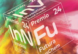
XVIII Edición de los Premios Suschem Jóvenes Investigadores Químicos.
Si deseas recibir información sobre nuestras actividades y las noticias más destacadas del sector, pero, además, quieres beneficiarte de todas las ventajas ser miembro afiliado de SusChem - ESPAÑA, no dudes en solicitar tu afiliación a nuestra plataforma.
¡Quiero afiliarme!

The aim of the conference is to review the advances in the field of electronic devices, according to the following topics:
Horizontal topics (techniques and processes)
H1. Materials and processing technology
Manufacturing techniques for bulk or 2D layered materials (LPE, MBE, MOVPE, CVD, ALD ...). Development of semiconductor materials: carbon-based materials: graphene, CNT, fibers... New organic semiconductors. Technological processes and their simulation: bulk substrates treatment, photolithography, e-beam lithography, etching, FIB, diffusion, ion implantation, insulator and metal deposition, ohmic contacts, etc. Ink-jet, 3D, and other new printing techniques for electronic devices.
H2. Device modelling and simulation
Statistical, numerical or analytical models for electronic, optical, or physical device aspects. Physical and circuital device models and their interconnection.
H3. Characterization and reliability
Physical and chemical characterization of electronic materials: SIMS, XPS, photoluminescence, Hall effect, XRD, SEM, TEM, STM, AFM, AES, RBS, etc. Electrical and optical device characterization: quantum efficiency, I-V, C-V, impedance, TLM, etc. Device reliability, fault analysis, electromigration, real-time and fast degradation experiments, etc.
Vertical Topics (Device Types)
V1. Sensors, actuators, and micro/nano systems
Structures and their integration into devices for sensors, actuators, micro/nanosystems, and MEMS/NEMS. It includes sensors for physical, chemical, gas, electrochemical, mass ... detection. Integrated sensors. Hybrid integration with optical components. Energy harvesting. Electronic noses.
V2. Photovoltaic and optoelectronic/photonics devices and displays
Single crystal technologies (Si, III-V), thin film technologies (chalcogenides, a-Si, perovskites...), organic PV, third generation-based concepts. Optoelectronic devices: LEDs, lasers, optical modulators, photodiodes, CMOS, or CCD array detectors. Photonic Crystals structures. Displays: TFT, LCD, OLEDs...
V3. Biomedical devices and Lab-on-Chip
Sensors for biomedical detection. SPR. DNA chips. Micro-optofluidics. Micro- and nano separation technologies. Micro- and nano total analysis systems (uTAS, nTAS). Biological fuel-cells. Implantable medical devices and drug delivery devices. Medical diagnostic microsystem. Bioelectronics applications.
V4. New device concepts: quantum devices, nano-devices, RF, microwave and power devices
New functional devices based on nanostructures: nanotubes, nanowires, quantum dots, graphene, etc. Magnetic, nano-photonic, spintronic, and molecular devices. Memristive switching devices. Devices for micro-energy harvesting. Terahertz operating devices. Discrete and integrated devices for high power/voltage/current operation, including FETs, HBTs for high power, RF, microwave and integrated switches, capacitors, inductors, and components for batteries.
SS. Special session: Memristors
Memristors, or memory resistors, are a type of electronic device that can store and process information in a way that mimics the synaptic behavior of the human brain. As such, memristors hold great potential for revolutionizing computing and artificial intelligence. Over the past few years, there have been significant advances in the development of memristor-based technologies, from novel materials and fabrication techniques to applications in neuromorphic computing, analog computing, and beyond. In this session, we will hear from leading researchers in the field about the latest breakthroughs in memristor science and engineering, and explore the exciting possibilities that lie ahead.
XVIII Edición de los Premios Suschem Jóvenes Investigadores Químicos.
Una iniciativa del GT Interplataformas de Economía Circular.
Sistema de ofertas y demandas tecnológicas de SusChem-España con la química sostenible.
DATOS CLAVE I+D+i DEL SECTOR QUÍMICO
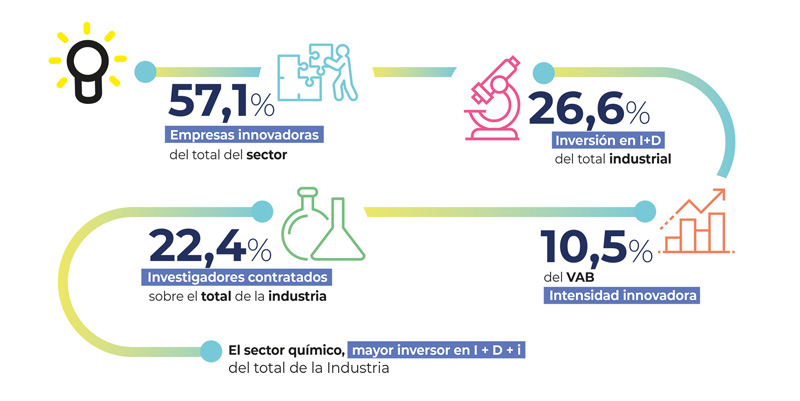

Principales Indicadores de I+D+i del Sector Químico Español. Sector lider que invierte anualmente más de 1.800 Millones de Euros en I+D+i.